
PCB Inspection
Process: Inspection

Inspection Area: 800 x 750mm
Minimum Detectable PCB Feature Size: 30μm
PCB Correction for Precision Manufacturing
Our PCB scanning and stencil data correction process addresses the critical challenge in Electronics Manufacturing: misalignment between flawless computer-generated PCB design data and the variations present in real-world manufactured boards. Even minor discrepancies between design and production can compromise stencil accuracy, resulting in poor solder paste deposition, reduced yield and higher operational costs.
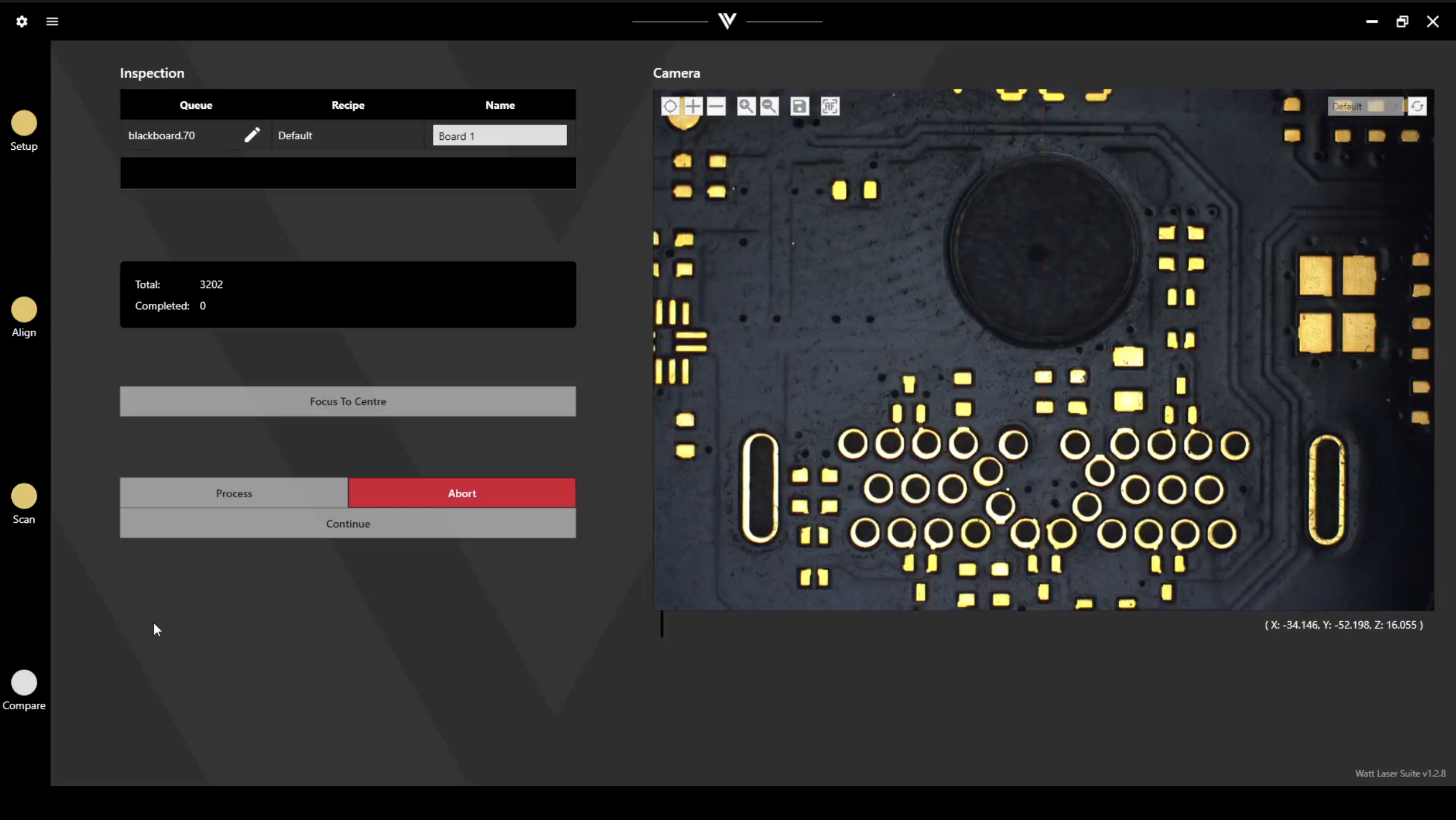
This software-driven process leverages Watt Laser’s high-resolution optical systems to perform detailed grid scans across one or multiple PCBs. By analysing physical features within strict tolerance bands, the system builds a comprehensive correction map. This map identifies where production boards deviate from design intent and applies precise, data-driven adjustments to the stencil mask files before fabrication. Larger PCB sample sets further improve accuracy by providing stronger statistical baselines for correction.
Once processed, the application generates a data report for the user, detailing every data point retrieved. This enables direct comparison between the scanned PCBs and the original CAD data, as well as cross-analysis between different boards in a sample set. Such reporting provides manufacturers with actionable insights into overall process conformity, highlighting both localised misalignments and broader production trends.
By enabling post-design correction of stencil data, our PCB scanning application not only ensures that apertures align more accurately with PCB pads but also allows for the reduction of aperture size tolerances. This translates into tighter process control, cleaner solder printing, reduced rework and significant cost savings on stencil material and manufacturing overhead. In short, the system elevates stencil accuracy to meet real-world conditions, improving quality and efficiency across the entire PCB assembly workflow.

Adam Steven
Project lead

Why it matters?
This project represents more than just a technical solution; it highlights our commitment to solving practical manufacturing challenges with creativity and precision. PCB manufacturing is inherently complex, and traditional stencil data often fails to account for the subtle variations that emerge in real-world production. By designing a system that intelligently bridges the gap between digital perfection and physical reality, our team has not only reduced defects and costs but also demonstrated how innovation can directly improve manufacturing outcomes.
Speak to our team today
We’d love to chat to you about our laser solutions and how we can work together.